
Maskless Arbitrary Writing of Molecular Tunnel Junctions
| author | Hyo Jae Yoon |
|---|---|
| Homepage | https://hyojaeyoon.wixsite.com/omml |
| journal | ACS Appl. Mater. Interfaces, Article ASAP |
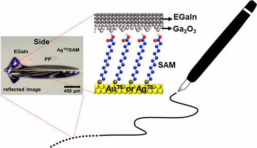
Since fabricating geometrically well-defined, noninvasive, and compliant electrical contacts over molecular monolayers is difficult, creating molecular-scale electronic devices that function in high yield with good reproducibility is challenging. Moreover, none of the previously reported methods to form organic–electrode contacts at the nanometer and micrometer scales have resulted in directly addressable contacts in an untethered form under ambient conditions without the use of cumbersome equipment and nanolithography. Here we show that in situ encapsulation of a liquid metal (eutectic Ga–In alloy) microelectrode, which is used for junction formation, with a convenient photocurable polymeric scaffold enables untethering of the electrode and direct writing of arbitrary arrays of high-yielding molecular junctions under ambient conditions in a maskless fashion. The formed junctions function in quantitative yields and can afford tunneling currents with high reproducibility; they also function at low temperatures and under bent. The results reported here promise a massively parallel printing technology to construct integrated circuits based on molecular junctions with soft top contacts.
« Prev Recent Progress in the Chemistry of Pyridazinones for Functio...
 Recent Progress in the Chemistry of Pyridazinones for Functio...
2018.01.31by Manager
〈
Single Component Organic Solar Cells Based on Oligothiophene-... Next »
 Single Component Organic Solar Cells Based on Oligothiophene-...
2017.10.23by Manager
〉
-
Read More
Molecular Role of Ca2+ and Hard Divalent Metal Cations on Accelerated Fibrillation and Interfibrillar Aggregation of α-Synuclein
Hugh I. Kimhttps://sites.google.com/site/hughkimgroup/α-Synuclein (αSyn) is an intrinsically disordered protein, the aggregation of which is highly related to the pathology of diverse α-synucleinopathies. Various hard divalent metal cations have been shown to affect αSyn...Date2018.01.31 ByManager Views1788 -
Read More
Supramolecular Modulation of Structural Polymorphism in Pathogenic α-Synuclein Fibrils Using Cu(II) Coordination
Hugh I. Kimhttp://Angew. Chem. Int. Ed. 2018 (DOI: 10.1002/anie.201712286)Structural variation of α-synuclein (αSyn) fibrils has been linked to the diverse etiologies of synucleinopathies. However, little is known about what specific mechanism provides αSyn fibrils with pathologic features. Herei...Date2018.01.31 ByManager Views1376 -
Read More
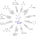
Recent Progress in the Chemistry of Pyridazinones for Functional Group Transformations
Hyo Jae Yoonhttps://hyojaeyoon.wixsite.com/ommlWhile N-hetereocycles have received significant attention in organic synthesis and other research fields, the chemistry of pyridazine, six-membered aromatic ring with adjacent two nitrogen atoms, and its derivatives has been relatively littl...Date2018.01.31 ByManager Views57076 -
Read More
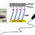
Maskless Arbitrary Writing of Molecular Tunnel Junctions
Hyo Jae Yoonhttps://hyojaeyoon.wixsite.com/ommlSince fabricating geometrically well-defined, noninvasive, and compliant electrical contacts over molecular monolayers is difficult, creating molecular-scale electronic devices that function in high yield with good reproducibility is challe...Date2018.01.31 ByManager Views1551 -
Read More
Single Component Organic Solar Cells Based on Oligothiophene-Fullerene Conjugate
Han Young Woohttp://www.ooml.korea.ac.kr/A new donor (D)–acceptor (A) conjugate, benzodithiophene-rhodanine–[6,6]-phenyl-C61 butyric acid methyl ester (BDTRh–PCBM) comprising three covalently linked blocks, one of p-type oligothiophene containing BDTRh moieties an...Date2017.10.23 ByManager Views2605 -
Read More
Lanthanide metal-assisted synthesis of rhombic dodecahedral MNi (M=Ir and Pt) nanoframes toward efficient oxygen evolution catalysis
Kwangyeol Leehttp://nanolab.korea.ac.kr/Mixed metal alloy nanoframeworks have shown a great promise as electrocatalysts in water electrolyzers and fuel cells. Although a limited number of mixed metal alloy nanoframeworks have been synthesized through phase segregation of alloy pha...Date2017.10.23 ByManager Views2425 -
Read More
Radially Phase Segregated PtCu@PtCuNi Dendrite@Frame Nanocatalyst for the Oxygen Reduction Reaction
Kwangyeol Leehttp://nanolab.korea.ac.kr/Pt-based alloy nanoframes have shown a great potential as electrocatalysts toward oxygen reduction reaction (ORR) in fuel cells. However, the intrinsically infirm nanoframes could be severely deformed during extended electro-cyclings, which ...Date2017.10.13 ByManager Views1591 -
Read More
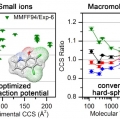
Collision Cross Sections and Ion Structures: Development of a General Calculation Method via High-quality Ion Mobility Measurements and Theoretical Modeling
Hugh I. Kimhttps://sites.google.com/site/hughkimgroup/Ion mobility mass spectrometry (IM-MS) has become an important tool for the structural investigation of ions in the gas phase. Accurate theoretical evaluation of ion collision cross sections (CCSs) is essential for the effective application...Date2017.10.13 ByManager Views1975 -
Read More
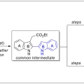
Previous Article Next Article Table of Contents Total Syntheses of Arcyriaflavin A and Calothrixin B Using 2,2′-Bisindole-3-acetic Acid Derivative as a Common Intermediate
Cheol-Hong Cheonhttps://sites.google.com/site/cheonresearchlab/A new protocol for the synthesis of 2,2′-bisindole-3-acetic acid derivatives from aldimines derived from 2-aminocinnamic acid derivatives and indole-2-carboxaldehyde was developed via a cyanide-catalyzed imino-Stetter reaction. With th...Date2017.10.10 ByManager Views1609 -
Read More
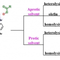
Synthesis, Characterization, and Efficient Catalytic Activities of a Nickel(II) Porphyrin: Remarkable Solvent and Substrate Effects on Participation of Multiple Active Oxidants
Suk Joong Leehttp://inmlab.korea.ac.kr/A new nickel(II) porphyrin complex, [NiII(porp)] (1), has been synthesized and characterized by 1H NMR, 13C NMR and mass spectrometry analysis. This NiII porphyrin complex 1 quantitatively catalyzed the epoxidation reaction of a wide range o...Date2017.09.26 ByManager Views1649 -
Read More
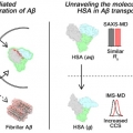
Molecular Insights into Human Serum Albumin as a Receptor of Amyloid-β in the Extracellular Region
Hugh I. Kimhttps://sites.google.com/site/hughkimgroup/Regulation of amyloid-β (Aβ) aggregation by metal ions and proteins is essential for understanding the pathology of Alzheimer’s disease (AD). Human serum albumin (HSA), a regulator of metal and protein transportation, can mod...Date2017.09.25 ByManager Views2625 -
Read More
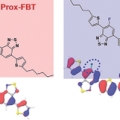
Two Regioisomeric π-Conjugated Small Molecules: Synthesis, Photophysical, Packing and Optoelectronic Properties
Dong Hoon Choi, Han Young WooTwo regioisomeric D1-A-D-A-D1 type π-conjugated molecules (1,4-bis{5-[4-(5-fluoro-7-(5-hexylthiophen-2-yl)benzo[c][1,2,5]thiadiazole)]thiophen-2-yl}-2,5-bis(hexyldecyloxy)benzene (Prox-FBT) and 1,4-bis{5-[4-(6-fluoro-7-(5-hexylthioph...Date2017.09.25 ByManager Views1593 -
Read More
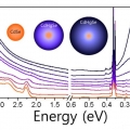
Major Electronic Transition Shift from Bandgap to Localized Surface Plasmon Resonance in CdxHg1-xSe Alloy Nanocrystals
Kwang Seob Jeonghttps://sites.google.com/site/ksjkulab/CdxHg1-xSe alloy nanocrystals are obtained from CdSe semiconductor nanocrystals via cation exchange. By varying the composition during the exchange process, the CdxHg1-xSe alloy nanocrystals offer a widely tunable electronic transition from ...Date2017.09.25 ByManager Views2575 -
Read More
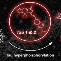
Rational Design of In Vivo Tau Tangle-Selective Near Infrared Fluorophores: Expanding the BODIPY Universe
Jong Seung Kimhttp://orgchem.korea.ac.kr/The elucidation of the cause of Alzheimer’s disease remains one of the greatest questions in neurodegenerative research. The lack of highly reliable low-cost sensors to study the structural changes in key proteins during the progres-si...Date2017.09.25 ByManager Views4694 -
Read More
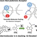
Achieving Highly Efficient Nonfullerene Organic Solar Cells with Improved Intermolecular Interaction and Open-Circuit Voltage
Han Young Woohttp://www.ooml.korea.ac.kr/A new acceptor–donor–acceptor-structured nonfullerene acceptor ITCC (3,9-bis(4-(1,1-dicyanomethylene)-3-methylene-2-oxo-cyclopenta[b]thiophen)-5,5,11,11-tetrakis(4-hexylphenyl)-dithieno[2,3-d′:2,3-d′]-s-indaceno[1,2-b...Date2017.09.25 ByManager Views2173 -
Read More
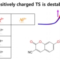
Ionic effect on the excited-state proton transfer reactions in aqueous solutions
Sungnam Parkhttp://ultrafastspec.wixsite.com/sparkProton dissociation (PD) reactions of weak acids and proton transfer (PT) processes in aqueous solution are strongly influenced by ions. However, a detailed molecular picture that describes how ions affect the rates for PD and PT processes i...Date2017.09.25 ByManager Views5740 -
Read More
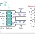
A conductive porous organic polymer with superprotonic conductivity of a Nafion-type electrolyte
Chang Seop Honghttps://www.immlab.korea.ac.kr/As potential solid electrolytes in fuel cells, porous organic polymers show compelling proton conductivities (up to ∼10−2 S cm−1), but even higher performance is required for real applications. In this work, we prepared a bip...Date2017.09.25 ByManager Views1990 -
Read More
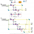
Quantum optical measurements with undetected photons through vacuum field indistinguishability
Minhaeng Chohttp://cmsd.ibs.re.kr/html/cmsd_en/Quantum spectroscopy and imaging with undetected idler photons have been demonstrated by measuring one-photon interference between the corresponding entangled signal fields from two spontaneous parametric down conversion (SPDC) crystals. In ...Date2017.09.25 ByManager Views3263 -
Read More
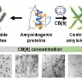
Nanoscale Control of Amyloid Self-Assembly Using Protein Phase Transfer by Host-Guest Chemistry
Hugh I. Kimhttps://sites.google.com/site/hughkimgroup/Amyloid fibrils have recently been highlighted for their diverse applications as functional nanomaterials in modern chemistry. However, tight control to obtain a targeted fibril length with low heterogeneity has not been achieved because of ...Date2017.07.21 ByManager Views3918 -
Read More
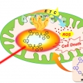
A Mitochondria-targeted Cryptocyanine-Based Photothermogenic Photosensitizer
Jong Seung Kimhttp://J. Am. Chem. Soc., Just Accepted Manuscript(DOI: 10.1021/jacs.7b04263)Cryptocyanine-based probes exhibit highly efficient photothermal conversion and represent a new class of photothermal agents for use in photothermal therapy (PTT). With the thermal susceptibility of mitochondria in mind, we have prepared a m...Date2017.06.27 ByManager Views1808
Designed by sketchbooks.co.kr / sketchbook5 board skin